Intel and Terafab have announced a partnership to develop advanced chip packaging facilities in the United States, a move that signals both companies are serious about reshoring critical semiconductor infrastructure. The deal, disclosed this week, will see Intel provide technical expertise and process technology while Terafab builds out physical capacity at its planned Arizona campus.
Why Packaging Matters Now
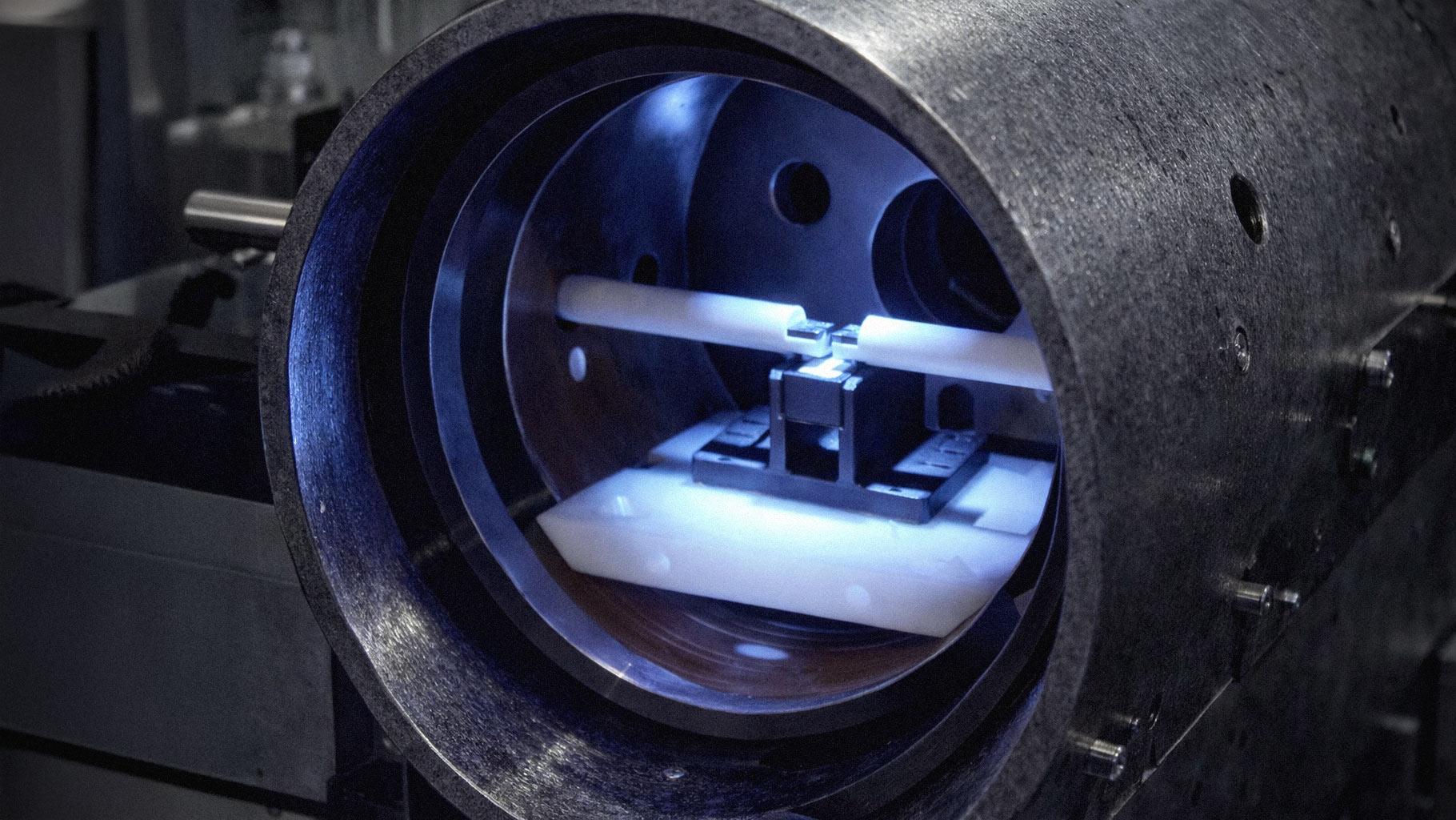
For decades, the semiconductor industry treated chip packaging as an afterthought. The real action was in fabrication, shrinking transistors down to impossibly small dimensions. But that calculus has shifted. As chiplet architectures become standard, the ability to connect multiple silicon dies into a single package has become just as important as manufacturing the dies themselves.
Intel has invested heavily in this area with its Foveros and EMIB technologies. The problem is that most advanced packaging still happens in Taiwan and South Korea. The partnership with Terafab represents an attempt to change that geography.
As we covered earlier this year, Terafab wants to build America's chip future before it's too late. The company has positioned itself as a domestically focused foundry alternative, targeting customers who need supply chain certainty more than bleeding-edge nodes.
The Strategic Calculus
For Intel, the partnership serves multiple purposes. The company has struggled to compete with TSMC on leading-edge fabrication, but advanced packaging represents a domain where it can still differentiate. Sharing that expertise with a domestic partner creates an ecosystem that could eventually feed back into Intel's own foundry business.
There's also the matter of government support. The CHIPS and Science Act has made billions available for domestic semiconductor manufacturing, and projects with clear national security implications tend to move to the front of the line. A U.S.-based advanced packaging facility would reduce dependence on Asian suppliers for a critical step in the production chain.
Terafab gains access to proven technology without having to develop it from scratch. Building a packaging operation is expensive, but licensing established processes shortens the timeline considerably.
What This Means for the Industry
The deal reflects a broader trend in semiconductor manufacturing. Companies are no longer optimizing purely for cost or performance. Resilience has entered the equation, and that changes how supply chains get structured.
This matters beyond chips. The hidden bottlenecks in chip manufacturing extend across materials, equipment, and specialized processes. Packaging is one piece of a larger puzzle that includes photomasks, advanced substrates, and high-purity chemicals.
Whether the Intel-Terafab partnership succeeds will depend on execution. Building semiconductor facilities is notoriously difficult, and timelines slip constantly. Intel's own struggles with new fabs offer a cautionary tale. But the strategic logic is sound. The companies that figure out domestic advanced packaging will have leverage that matters in ways that weren't obvious five years ago.
The first Terafab packaging lines are expected to come online in 2027, assuming construction proceeds on schedule.